Layout Parameter Extraction and Analysis Tool
Total support for a wide range of characteristic analysis from pixel cells to the entire panel
- High-accuracy parasitic resistance and capacitance extraction using 2D and 3D solvers
High-speed, high-accuracy parasitic extraction for pixel cell layout from top-level panel wiring - Provides analysis solutions for each FPD specific field such as voltage drop analysis

Resistance Extraction Tool for FPD
SX-Meister FineAcres
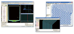
■High-speed and high-accuracy extraction of resistance values from figures of all shapes
- High-speed calculation of wiring resistance value by FEM
Supports complex shapes including any-angle figures, arcs, and slits - Electrode resistance distribution measurement by multipoint continuous measurement


Capacitance Extraction Tool for FPD
SX-Meister FineQap
■Full-panel scale high-accuracy, high-speed wiring capacitance extraction
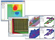
- BEM 3D capacitance extraction engine
- Parasitic extraction of wiring for large-scale and high-aspect ratio panels
Extracted model generation from layout data and wiring section parameters
Supports any angle wiring and multi-layer wiring
Supports non-flattening process
Supports floating metal - Check process structure and extraction results by 3D viewer


Resistance and Capacitance Extraction Tool for FPD
SX-Meister FineResQ
■Extraction of wiring resistance and capacitance with high accuracy and high speed on a panel scale
- Optimal algorithm that enables high-accuracy and high-speed extraction of resistance and capacitance
- Parasitic extraction of large-scale and high-aspect ratio panel wiring
- Outputs wiring parasitic information to support circuit analysis
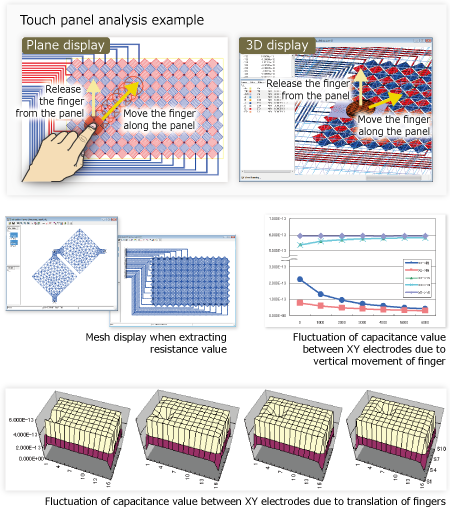
- Applicable to characteristic analysis of various touch panels


Voltage Drop and Current Density Analysis Tool for OLED Panels and Lighting Design
SX-Meister FineVolt
■Voltage Drop and Current Density Analysis Tool for OLED Panels and Lighting Design
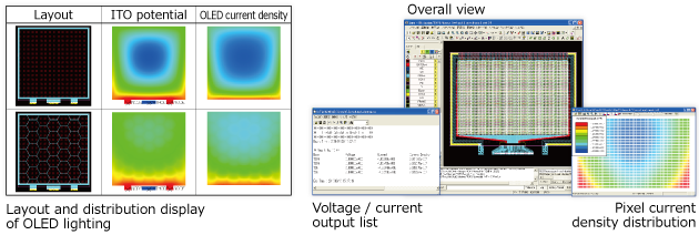
- Calculates and displays the voltage drop and current density distribution of the wiring inside the panel
- Calculates the current for each pixel in consideration of the voltage drop, and displays the current density of each pixel
- Automatic recognition of wiring and devices
- Device model
Spice model (aSi / LTPS TFT)
Impoert I-V characteristics (TFT/organic EL layer)


 Download